The Evolution of VLSI and its Role in the AI Era
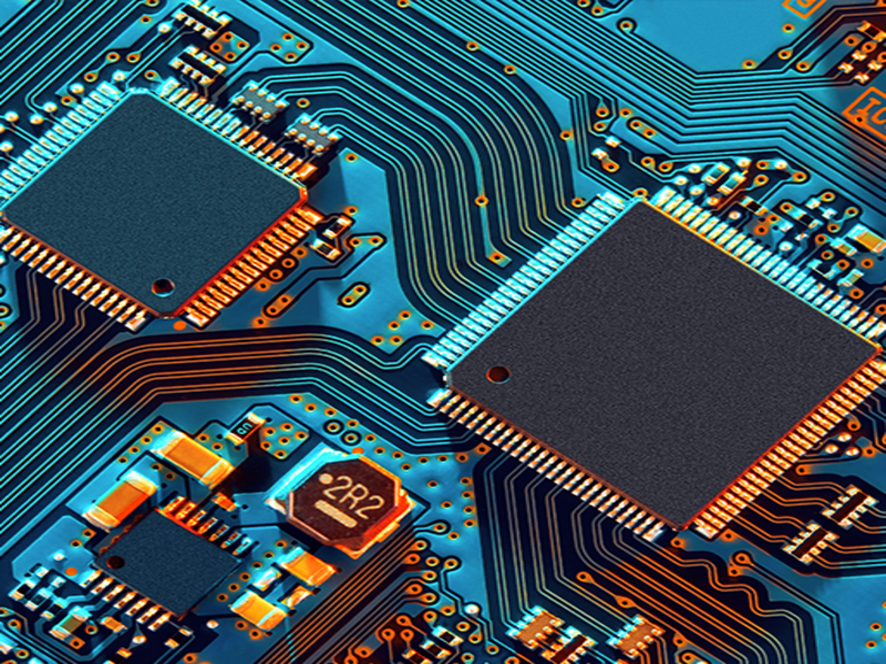
The invention of the integrated circuit (IC) by Jack Kilby and Robert Noyce in 1958 marked the beginning of VLSI technology evolution, starting with Small-Scale Integration (SSI) in the 1960s. Bulky vacuum tubes gave way to integrated circuits (ICs) at this point. Thousands of transistors were merged into a single chip via Medium-Scale Integration (MSI), which was followed by Large-Scale Integration (LSI). The groundwork for contemporary computing was laid in the 1980s with the introduction of VLSI, which allowed for the integration of tens of thousands to millions of transistors onto a single chip. In the 1990s, Ultra-Large-Scale Integration (ULSI) enabled billions of transistors on a single chip. This breakthrough led to the creation of complex systems like the Pentium microprocessor. VLSI technology was further advanced by the emergence of System-on-Chip (SoC) designs in the 2000s, which enabled modular chip integration and vertical stacking, improving performance and lowering power consumption, especially in applications using artificial intelligence and machine learning.
In the AI era, VLSI technology is essential because it allows real-time processing on wearables and robots. It manages the processing requirements of AI algorithms, facilitating developments in robots, driverless cars, and smart cities. Additionally, VLSI supports the infrastructure of data centres by offering enormous parallel processing power for training complex AI models. Innovation in a variety of industries is fuelled by the ongoing development of VLSI, which guarantees that computer systems can satisfy the expanding requirements of AI applications.
The VLSI industry in India presents promising career opportunities for students, particularly in the rapidly expanding semiconductor sector. The Government of India has launched several initiatives to enhance domestic manufacturing and design capabilities, like the Semicon India Programme (https://www.semiconindia.org), which has an investment of ₹76,000 crore ($10 billion); the Production Linked Incentive (PLI) Scheme (https://www.india.gov.in/production-linked-incentive-pli-scheme), which offers incentives to international chipmakers; and the Design Linked Incentive (DLI) Scheme (https://chips-dli.gov.in/), which has an investment of ₹1,500 crore ($200 million) for chip design start-ups. With the expansion of multinational semiconductor companies like Vedanta, Foxconn, Micron, Intel, Qualcomm, and NVIDIA in India, these investments are anticipated to generate more than 20,000 direct and indirect skilled jobs in VLSI design and verification.
The Department of Electronics and Communication Engineering at Presidency School of Engineering offers B.Tech. Electronics & Communication Engineering,and B.Tech. VLSI and M.Tech. Embedded Systems & VLSI, which will enable students to explore roles like VLSI design engineer, verification engineer, physical design engineer, and applications engineer, offering competitive salaries.
Dr. Rajiv Ranjan Singh
Professor & HoD, Department of Electronics and Communication Engineering / Electrical and Electronics Engineering, Presidency University, Bengaluru


 Rajanukunte, Yelahanka, Bengaluru, Karnataka, Pin: 560119, India
 +91 9022092222